Innovotek -News & BLOG
A blog about the news of the latest technology developments, breaking technology news, Innovotek Latest news and information tutorials on how to.
Asic design doesn’t need to be a rich man’s game

- Font size: Larger Smaller
- Hits: 7647
- 0 Comments
- Subscribe to this entry
- Bookmark
 Anecdotal mentions of hefty sums of more than $25m just to buy one mask set and total design costs reaching into many hundred million dollars, seem to mark out ASIC design as a rich person’s game. But these figures are only for the leading-edge processes typically used for high volume consumer products like smartphones.
For internet of things (IoT) applications, where integration levels are lower and the need to interface with the real world mandates the use of analogue circuitry, mature “more than Moore” process technologies are more suitable. Here the costs and risks of using ASIC technology are very different.
ASIC design and production has actually become cheaper for many projects, to the point that many people who used to believe field-programmable gate arrays or microcontrollers coupled with discrete analogue devices were their only options are finding out that the dedicated ASIC approach is more cost-effective.
The key is to choose the appropriate design tools and more importantly process technology; take advantage of relatively inexpensive, mature process technology; and make use of widely availability free or low cost IP.
The benefits of ASICs include performance, lower power, higher voltages, reduced footprint/bill of materials and thus increased reliability. Also important, they offer higher IP security, as an ASIC can be harder to reverse engineer than a microcontroller or FPGA design, where the IP is stored in easy-to-read memory.
Many foundries can provide a range of pre-characterised silicon IP. The use of such IP blocks is commonplace in the digital world. For example, companies like ARM and Imagination Technologies offer a range of functional blocks such as microcontrollers, many of which are suited to use in these mixed-signal technologies, especially in IoT applications.
Analogue circuit blocks like comparators, operational amplifiers, bandgaps, analogue to digital and digital to analogue converters greatly reduce design time and risk for the designer.
These older processes also offer support for higher voltage operation, which means they are common choices for mixed-signal designs where analogue accuracy is important. Older processes also make sense for applications where there is a need to work in or control higher voltages, such as automotive, industrial control or power management applications.
Some foundries can even tailor their foundry processes to meet specific product or application requirements. Plessey Semiconductors, for example, has a unique low power process developed specifically for implanted medical devices such as pacemakers.
Costs and risks in mask and wafer production can be further reduced by using multi-project wafer (MPW) services from organizations such as EUROPRACTICE IC Manufacturing. Where small quantities of chips are needed for evaluation/qualification or small production runs, several designs can be incorporated in a single mask set, as shown in the Figure 1 (courtesy of MOSIS).
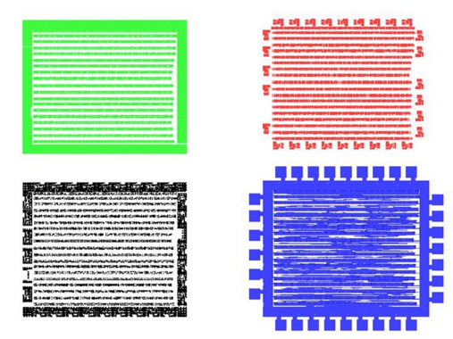
Figure 2. Multi-Layer Mask (MLM) (Source: XFAB)
Customers typically order 40 devices for evaluation before going to the expense of a dedicated mask set, but up to 1000 devices of any one design could be produced in a single MPW run. MPW costs are just a fraction of those needed for a complete set of dedicated masks and wafers, as customers only pay for the proportion of the wafer that their devices occupy. Most major foundries support multi-project wafer services.
A variation on this theme to further reduce the cost of production mask sets, offered by XFAB, is for several process layers to be drawn on the same mask. Figure 2 shows 4 layers on one mask, cutting mask costs by as much as 70%. This is known as Multi-Layer Mask or MLM.
It’s important to remember that neither older processes nor MPW services inhibit leading-edge analogue design. The first single-chip Bluetooth transceiver, as shown in Figure 3, was developed in the late 1990s by a start-up using a 0.35um CMOS process.
More recently, when another Cambridge start-up was developing a new generation of communications ASICs to exploit the now free to use unlicensed spectrum previously used by analogue TV transmission they turned not to 14nm or even 40nm, but the now mature 90nm process node. The relatively low wafer cost coupled with excellent yield ensured the device offered sufficiently low pricing for the commercially sensitive high volume application, coupled with good analogue performance and maturity of process needed to ensure right first time design.
Wide availability of low cost device assembly and test services complete the manufacturing supply chain, ensuring fully functioning packaged, tested chips can be delivered easily and cheaply.
The use of mature processes brings tool cost down. There is no need to buy expensive leading-edge design tools intended for advanced nanometre-scale SoC design, as they contain many features that are unnecessary for design in the mature nodes.
For example, you need a far more complex and thus expensive design tool to perform simulation, layout or verification of a billion gate design in a recently released process node than you do for a relatively simple mixed-signal circuit in a mature process, where the gate count may range in the 10s of 1000s, and most of the analogue circuits are IP blocks provided by the foundry and used many times before.
Low cost design tools such as the Tanner AMS IC design flow (formerly Tanner EDA HiPer Silicon), which was used extensively in both the above examples, have support for HDL digital design, synthesis and place and route together with support for full custom analogue design, allowing engineers to move into mixed-signal chip design on mature processes cost-effectively and easily.
For the analogue side of the design, low cost or even free-to-use open source tools bring many of the benefits that high-end tools offer without unnecessary features (and thus cost). Low cost tools are often easier to use because they do not put advanced features in the way. However, this does not mean they lack the functionality or capability of the high-end tools for analogue and mixed-signal design.
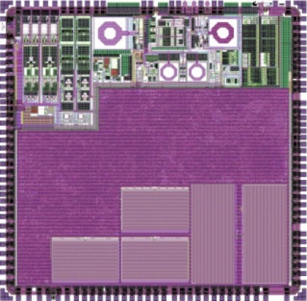
Bluetooth Transceiver (Source: CSR)
Another major factor in the choice of design tools is the easy availability of the PDKs needed for accurate and efficient design. This is made easier by the wide adoption in the industry of the emerging interoperable PDK or iPDK standard. iPDKs are developed by most foundries today and are designed to work with all the major IC design tools.
These iPDKs not only contain the basic process related data like simulation models and process layers, but also complex device generation macros known as P-Cells (parameterized cells). It used to be that most tool vendors used proprietary languages for their P-Cells and so foundries had to choose which tool vendors to support. Now, with most tool vendors supporting Python as the language used in their P-Cells, foundries can support all the major tool vendors with one PDK.
Low cost tools have one further saving on their side. Ongoing support costs are a major feature of high-end tools. Dealing with the complexities of setting up and maintaining such leading edge SoC design flows often demands the support of a dedicated CAD department or the involvement of expensive maintenance contracts. If you are working with a smaller AMS design team you have to ask yourself whether you need to incur the cost of this type of CAD support, especially when more cost-effective tools are designed to work straight out of the box.
For mature processes, IC design is becoming more accessible thanks to the ready availability of production capacity and lower non-recurrent engineering costs made possible by low cost tools and lower-priced processes. There is no need to feel that your only options are FPGAs or discrete micros with board-level analogue circuits. Mature processes allow you to reduce costs and improve performance by putting the key differentiating elements of your product design into one IC. Custom ICs are no longer the preserve of those companies with deep pockets.