INNOVOTEK
A blog about the news of the latest technology developments, breaking technology news, Innovotek Latest news and information tutorials on how to.
General Partitioning Guidelines for Validation of Large ASIC Designs On FPGA
- Font size: Larger Smaller
- Hits: 52821
- 0 Comments
- Subscribe to this entry
- Bookmark
 Today, a lot of the system-on-chip (SoC) designs depend on Field-Programmable Gate Arrays (FPGAs) as a way to accelerate verification, early start of software development and validate the whole system before committing to silicon. This is done primarily to meet time-to-market demands. Today's FPGAs have the capability to contain a complex and large system-level design. However, in some cases, there is a requirement for these designs to be partitioned among several FPGAs for validation or prototyping. But, splitting the design into several FPGAs can create various partitioning issues, especially for relatively large designs with complex connectivity. These issues could possibly be circumvented if certain guidelines are followed. This paper talks about the general partitioning challenges and the guidelines that can be followed to get past these issues.
Need For Partitioning:
As devices being prototyped on FPGAs are getting larger, following good design practices become important for all design flows. Adhering to recommended synchronous design practices makes designs more robust and easier to debug. Using an incremental compilation flow adds additional steps and requirements, but can provide significant benefits in design productivity by preserving the performance of critical blocks and reducing compilation time.
As the industry is getting competitive, time-to-market is one of the critical factors in SOC design flow. In order to minimize the time-to-market, there is a need to ensure first time full functional silicon avoiding re-spins, which can be achieved by extensive verification of design using FPGA prototyping. The first step in FPGA prototyping of a design is to analyze whether the design will fit in to a single FPGA. If the design is relatively small, it can be prototyped by just using a single FPGA. This reduces any need for design partitions or issues arising during or post partition. But for the modern intricate SOCs having large gate counts, a single FPGA might not be suitable to fit whole of the design. So there will be a need for partitioning the design in to number of FPGAs, and there will be partitioning issues that need to be taken care of, which will be discussed in the next section.
For some designs, even though it might seem that design will fit well in a single FPGA based on the ASIC gate count, but the design may still need to be partitioned because of the limited resources available on the target FPGA device. E.g. Memory or DSP-intensive ASICs frequently fall into this category of design.
Major considerations for partitioning:
Once it is established that a design partition is required, and there is a need to first estimate the number of FPGAs required for design prototype.
As a part of the partitioning process, following are the major concerns that one should keep in mind:
- The boundary of partition for a design is often guided by factors such as capacity of each FPGA and gate count of the partitioned design, availability of global clocks and number of asynchronous clock domains in the design etc. Hence, one should keep them in mind while deciding upon the blocks to be partitioned.
- Owing to the limitation on the number of available I/Os and interconnects in the FPGA, most ASIC designs may exceed the number of available I/Os in the FPGA. One might then want to either multiplex these pins before getting them to the interconnect pins or changing the partition boundary with reduced number of interconnecting nodes.
- As it is equally important to meet the timing of a partitioned design, hence the pin availability on FPGA is also constrained by this factor, making it necessary to refrain from poor pin assignment techniques.
- The presence of components such as memories, FIFO’s etc. which need mapping to FPGA resources such as RAM blocks etc. on each FPGA need special attention in the partitioning process. They are limited by the architecture of FPGA family and size of the device. This necessitates an intelligent demarcation to prevent exceeding the available resources as well as not over utilize them as it might lead to routing and timing issues.
Guidelines to avoid common partitioning issues:
Following are the general guidelines for partitioning of the design, which can eliminate the common partitioning issues and ensures better results.
1. Partition by design hierarchy and design files:
Design hierarchy must be considered during partitioning process as it can really simplify the process and eliminates the issue of re-partitioning of design for minor changes, more so in cases where the design is not mature enough and minor changes happen more often. Partitioning for such a less matured design is shown below in Fig.1 (a) and Fig.1 (b).
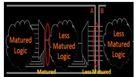
Fig.1 (a) Less Matured Partition Boundary
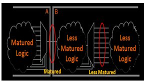
Fig.1 (b) Matured Partition Boundary
If a hierarchical instance is assigned as a design partition, the partition should also include the entities instantiated below that instance which are not defined as separate partitions. All the hierarchical partitions can be merged into a single partition, as long as they have the same immediate parent partition.
2. Partition by Functionality and Block Size:
Initially, the design can be partitioned along functional boundaries, as in a top-level block diagram, each block in itself is a design partition. Each block of a system can be considered as an independent module having more signal interaction internally than with other blocks. Keeping functional blocks together means that synthesis tools can optimize related logic as a whole, which can lead to improved optimization. Also, the number of partitions required needs to be estimated first in order to determine the size of each partition as compiling time depends upon the partition size. Too many partitions should also be avoided as it can reduce the quality of results by limiting optimization.
3. Partition by Clock Domain and Timing Criticality:
At the primitive stage of partitioning, clocks which feed the logic in each partition should be identified and if possible, clock domains should be kept within one partition. When a clock signal is isolated to one partition, it reduces dependence on other partitions for timing optimization as the logic in the other partitions is no longer dependent on the clock signal present in the current partition. Additionally, limiting the number of clocks within each partition simplifies the timing requirements for each partition during optimization. Logic which is implemented in design for clock domain transfers (such as a synchronization circuit) can be included inside the partition at one side of the domain transfer.
Isolating timing-critical logic from logic that is expected to meet its timing is always a good practice as it preserves the satisfactory results for non-critical partitions and focus optimization iterations on just the timing-critical portions of the design to minimize compilation time.
Also, if at all there are inter FPGA clocks i.e. there is a clock that originates in one FPGA and needs to be used by the logic in the other FPGA there can be issues regarding timings and data coherency. In cases like these it is advisable to route these clocks on the global clock pins on interconnects. However, these should be constrained for input and output offsets with respect to the clocks.
4. Partitioning Inputs and Outputs by Registers:
There are some input and output connections in design that are potentially timing-critical. Those connections can be partitioned using registers at partition boundaries, as boundary registers minimize the delays on inter-partition paths and prevent the need for cross-boundary logic optimizations. Partitioning of a design is shown below in Fig.2 having register at each partition boundary.
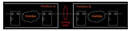
Fig.2 Design Partitioning By Register at Each Partition Boundary
As shown above, partitioning this way gives only routing delay, which needs to be considered for each register-to-register timing path and hence, timing paths between partitions are likely not timing-critical, and each partition can be placed independent of other partitions. Additionally, the partition boundary does not affect combinational logic optimization because each register-to-register logic path is contained within a single partition. Registering every partition output ensures that the input timing performance for each design block is controlled exclusively within the destination logic block.
5. Minimize Cross-Partition-Boundary I/O:
a) Minimizing the number of I/O paths crossing between partition boundaries makes partitions more independent for both logic and placement optimization. It is relatively more important for timing-critical and high-speed connections between partitions, especially in cases where the input and output of each partition is not registered. Slow connections that are not timing-critical are acceptable because they should not impact the overall timing performance of the design. But if there are timing-critical paths between partitions, inter-partition paths can be avoided by merging the partitions. The types of functions at the partition boundaries also govern the partitioning process.
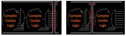
Fig.3 (a) Design with Poor Partition Boundary (b) Simplified Partition Boundary
A design partition with expansive partition boundary is shown above in Fig.3 (a) which can be simplified by minimizing the partition boundary as shown in Fig.3 (b). Partition quality of this design can be further improved, by adding registers to one or both sides of the cross-partition path subject to functionality adherence.
b) If interconnects across partitions are in same clock domain, partition boundary can also be simplified using I/O muxing approach which involves multiplexing a number of interconnect signals on a single interconnect pin. A design with heavy partition boundary is shown below in Fig.4 (a) whose partition boundary can be simplified by using I/O muxing technique as shown in Fig.4 (b).
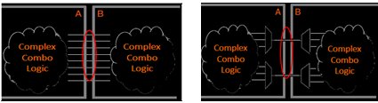
Fig.4 (a) Expansive Partition Boundary (b) Simplified Partition Boundary
The number of signals that can be multiplexed on a single interconnect pin depends on the frequency requirements of the design as for multiplexing X number of signals on a single pin reduces the maximum achievable frequency for the prototyped design by 1/X times (approx.).
c) Another way to minimize connections between partitions is to avoid using combinational “glue logic” between partitions by moving the logic to the partition at one end of the connection to keep more logic paths within one partition. A design is shown below in Fig.5, having glue logic between the partitions, which has a large partition boundary on the side of partition B.
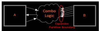
Fig.5 Design with Glue Logic between the Partitions
Now, the connections between the partitions can be minimized by moving the glue logic to partition B, as there are fewer connections on the side of partition A, which is shown below in Fig.6.
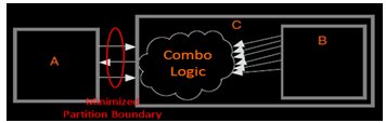
Fig.6 Design with Minimized Partition Boundary
Clearly, there are fewer I/O connections between partitions A and C than between partitions A and B which was shown earlier.
Conclusion:
Thus, by adhering to these simple guidelines for prototyping of relatively complex designs, we can decide the partition boundary, the number of partitions required, the type of device to be used as well as feasibility at an early stage of execution. It is rather beneficial to spend few hours in analyzing these attributes and coming to a decision at an early phase of the design than hitting a dead end in the execution phase and end up wasting crucial execution time.