Innovotek -News & BLOG
A blog about the news of the latest technology developments, breaking technology news, Innovotek Latest news and information tutorials on how to.
Integration of Design-for-Analysis in IC Layout Considerations to meet the Challenges of Shrinking Technology

- Font size: Larger Smaller
- Hits: 5764
- 0 Comments
- Subscribe to this entry
- Bookmark

Abstract:
This paper aims to emphasize on the importance of integrating design for failure analysis in the layout considerations during the IC development process. It will have a brief overview on the importance of failure analysis in an IC development process, followed by an understanding of the failure analysis methodologies in the industries. This leads us to the different considerations in the layout of ICs to facilitate failure analysis, and also the challenges in failure analysis with increasing complexities when the design approaches nano-electronics.
I. INTRODUCTION
The introduction of the System-on-a-Chip (SOC) and the increasing complexity of ASIC designs has made testability and analysis of Integrated Circuits (IC) more challenging. It has almost become a mandatory requirement to do a Design-for-Testability (DFT) and Design-for-Analysis (DFA) before the freezing of the ASIC design as the ability to test and analyze a complex design will bring about a shorter product cycle and faster time-to-market. In DFT, testability requirements are presented in various levels of an SOC. In terms of failure analysis, there are many techniques available to analyze the device for physical defects, from isolate the faulty behavior to the failing transistor and to capture the images at localized root cause in substrate level to understand the failing root cause. Unfortunately, even though there are many existing techniques available for failure analysis, the analysis may not always be possible. This is because the inevitable trend in IC design is that most of the time, in order to have a faster time to market, IC designers need to embed cores that are untested and are not manufactured in-house. There are inadequate considerations in the IC layout that make analyzability of an IC difficult or impossible. Furthermore, smaller technology nodes also brings about an increase in the metal layers of an IC, new materials in wafer manufacturing processes and different IC packages which pose greater challenges to failure analysis. These challenges lead to higher equipment cost, more experienced manpower required, longer analysis turn around time and difficulties in the analyzability of an IC. Even for reused IP which are proven in the design, process shrinking or backend process parameters shift may bring problems like higher leakage current and reduced reliability. Hence there is an increasing need to integrate failure analysis requirements with the IC development in an early phase. Strong interactions between development team and failure analysts are required to identify the possible bottlenecks from the very beginning and provide solutions with adequate layout considerations.
II. FAILURE ANALYSIS – THE DIFFERENT METHODOLOGIES
Failure analysis for integrated circuits is increasingly important and very much required for today’s complicated packaging and technology strategies. It is a process which requires the combination of analysis experiences, leading-edge equipment and techniques, and well defined failure analysis procedures to achieve fast turn around time for failure root cause findings. Failure analysis methodologies are important to the IC development process as it allows one to effectively identify the root cause of a design or process bug. The challenge of making rapid improvements in IC design and technology also requires the development of relevant failure analysis techniques. There are many analysis techniques and they can be generally divided into the 3 areas:
1. Chemical or physical preparation of the integrated circuits.
2. Fault localization of integrated circuit’s failing behavior.
3. Fault imaging of integrated circuits.
Chemical or physical preparation of the integrated circuit is the first step in the analysis of failing devices. The package has to be opened up either on the front or backside so as to allow further localization techniques to be carried out. Improved packaging techniques like Ball Grid Array (BGA) packaging had make the chemical or physical preparation increasingly challenging for failure analysis. This is an important process whereby one has to be careful not to destroy the failing signature and the electrical functions of a device.
Fault localization is the process where various techniques are used to isolate the defective areas on the die. Techniques like photoemission microscopy uses faint Infra-red radiation emitted by leakage current to localize the leakage site. Other techniques such as Thermal Induce Voltage Alteration (TIVA) uses the active approach whereby failure sites are located use a scanning ionizing beam, such as laser beams, to stimulate failures that are sensitive to carrier generation or thermal stimulation.[1] This allows one to reduce the area required for analysis and significantly save on the time required for failure analysis. The localized defect is then characterized with a view to understand the failure mechanism.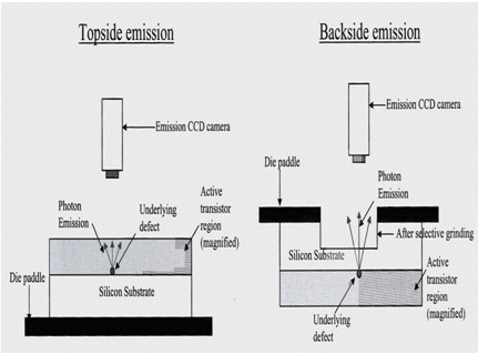
Fig. 1. Top and bottom photoemission setup in fault localization
The final step of failure analysis after fault localization is fault imaging. Failure analysis can only be completed once the root cause of the failure has been identified. Hence the defect must be imaged to prove the defective behavior. Optical microscopy is the obvious and most basic equipment for this purpose. However, with the complexity of microelectronics today, optical microscopy is of limited use. In order to achieve better resolution for imaging, microscopy is available using all kinds of beams: ultrasonic, electromagnetic (from infrared to x-ray) and particles like electrons and ions or near-field interactions with a stylus, as in scanning probe microscopy. All these imaging tools are equipped with CAD layout information for better navigation over the die. The FA processes can be generally summarized in the following table
| Chemical/Physical Preparation | Fault Localization | Fault Imaging |
| Front/Backside Decapsulation | Liquid Crystal Thermography | X-Ray Radiography |
| Cross Sectioning | Photo-emission Microscopy | Scanning Acoustic Microscopy |
| Focus Ion Beam | Thermal Induce Voltage Alteration | Scanning Electron Microscopy |
| Physical Delayering | Electron Beam Probing | Energy Dispersive X-ray Analysis |
| --- | Thermal Infra- red Microscopy | Scanning Force Microscopy |
Fig.2. Failure analysis methodologies used in IC development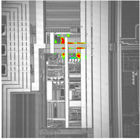 (a)
(a)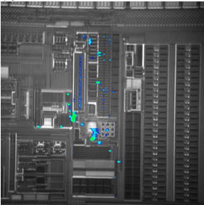 (b)
(b)
Fig. 3. TIVA imaging for leakage current on (a) front-side and (b) backside of an IC
III. Layout considerations to facilitate Failure analysis
With the understanding of failure analysis procedures, next comes the concern on the layout consideration in the design of an IC. Technology process is shrinking and designs are more complicated. It is quite a norm for a design to have 5 or more metal layers and hence the localization of any fault will be very difficult. Shrinking process and wafer fabrication process problem have huge impact on the product development cycle even with reuse IP. For a quick root cause findings, the layout of the IC has to be done with a design-for-analysis in mind. Without such considerations, it would be very difficult or impossible to find out the root cause of any failure. The following layout considerations are recommended in facilitating any failure analysis:
1. For any important nodes that would provide critical information, insert probing pads at the top layer to allow access to these nodes. For example, in the macro design of an embedded voltage regulator, a pad could be created to allow access for measurement of the band-gap voltage. Other important nodes like interfaces between macros, blocks, cells, scan flip-flop outputs should also be considered. Probing pad size should be 2um to 2um if possible for signals insensitive to additional capacitive loads. For static measurements needle probe requires a minimal area of 1.5um by 1.5um.
2. In IC product design, there is always a die size constraint whereby the die has to be designed to be as small as possible. To balance the trade-off between die size and analyzability, instead of creating probe pads which take up more space, some signal nodes which are critical are equipped with stacked via up to last possible metal layer so as to allow FIB pad to be deposited externally if there is a need to measure the critical nodes.
Fig.4. FIB pad deposition
3. In circuit modification using FIB, the ion beam uses gallium and other special gases for the deposition and removal of metal connections. Such deposition of metal contacts requires a minimal area so as to avoid shorting the surrounding signal lines. For example, in the creation of a FIB pad, the distance of the pad to neighboring signal lines shall have a minimum space of 300nm in both x and y direction to cater for FIB metal deposition for any possible modification. Furthermore, if the pads are in the bottom layers, one has to ensure that the layers on top on these pads are free from filling structures. Hence a fill exclude layer has to be applied above the pad areas for all layers in the remaining hierarchy up to the top layer.
4. Another consideration to facilitates analyzability is to have spare cells for any possibly modifications. The advantages of this flow are: All registers are included in the clock tree during clock tree synthesis; they are therefore fully balanced and functional in case of Engineering Change Order (ECO). All pins are connected, so it is also conceivable to include ECO registers in the existing scan chains. Routing is considered for all spare cells, which increases the chances of usability in case of metal fix.
5. For IC with embedded SRAMs, orientation of the SRAMs is important for analysis. Markers are required to mark the origin of the SRAM. For example, “F” markers located at proximity of the main SRAMs in the device can be used as part of the layout considerations. The markers help analysis by making alignment at the proximity of the memories possible, once resolution has been increased to zoom into particular areas of the chip. The markers are implemented by cutting 2 thin perpendicular strips in the LB power grid. Due to the grid alignment, the markers cannot be placed at any location but must be contained within a metal strip.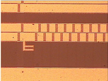
Fig.5. “F” markers for SRAM orientation
IV. CHALLENGES FOR FAILURE ANALYSIS In IC Design
There are many challenges looming in the future for failure analysis in the areas of fault isolation, inspection, and de-processing. In design for testability, it is increasingly essential to involve pre-designed and pre-verified modules or cores. The reuse of these designs effectively reduces the test time and cost for designs with multi-million gate system with a faster time-to-market. The International Sematech Product Analysis Forum has identified ten primary challenges for the future of the failure analysis in the semiconductor industry [4]:
- Localization and Electrical Characterization
- Deprocessing Techniques for New Materials
- System-on-a-Chip
- Imaging of Small Defects and Structures
- Detection and Characterization of Non-visual Defects
- Verification and Test
- Globally Dispersed Entities as Virtual Factory
- Fault Isolation and Simulation Software
- Cost of Failure Analysis
- Complexity and Volume of Data
For device failure analysis, the challenges can be generally divided into 2 areas. One is from a technical perspective, and the other from the business perspective. Technically, the challenges come in terms of the smaller feature size, new materials in wafer process, planarization in multi-level-metallization, new IC packages like BGA, CSP and flip chip.[8] These changes may render some of the traditional methodology to be obsolete and new revolutionized methods are required to come up fast to fill up such vacuums. The current trend in the industry is that the technology node is shrinking to 45 nm technology which will be commercially viable in 2008. With smaller node, more complexities will be involved in failure analysis. More sophisticated analysis machines and methodologies have to be developed to keep up with the pace. From the design perspective, more layout and design considerations will be required with strong inputs from the failure analysis experts.
From a business point of view, technology complexity in integrated circuit designs will inevitable incur high cost in the failure analysis of the product with higher investment on sophisticated equipment and manpower to ensure fast product development. The layout considerations will inevitably leads to bigger device size that pushes up the manufacturing prices. Hence the challenge is to keep a balance in terms of product costs and innovative product development improvements for the product to be profitable. The failure analysis requirement has consequences of large investment, techniques and skilled manpower. The demands for better failure analysis processes increase with complexity in integrated circuits technologies. If all the innovations for failure analysis are going to be realized, there will be a need to invest a much higher amount for failure analysis activities. An estimation of investment amount made by Christian Boit [8] on acquisition of failure analysis machines such as backside photoemission with IR detector, TIVA machine, FIB with CAD, and Laser absorption LSM, including license, training and manpower resources will cost about 10 million for product development. The ability to reduce this cost is another challenge in the process of keeping pace with newer technology.
There is a necessity for strong interaction between the development team and the failure analyst to get the most information out of the electrical testing for a quick failure analysis cycle time. For the purpose of reducing the increasing failure analysis cost and cycle time, failure analysis requires a new focus in the semiconductor industry. That is to integrate the failure analysis into integrated circuits development projects from early phase. Failure analysis will not be efficient if it is treated as just separate support to the semiconductor business. There is a need to cooperate and integrate into the development project in order to identify possible analysis bottlenecks from the beginning. This will leads to joint effort in analysis specification, identifying solutions, design workarounds and analysis method developments. It will also mean that prior to any technology project release, there will be a failure analysis risk evaluation. In a similar approach, prior to any packaging release, there will be an evaluation of failure analysis requirement on the packaging, and prior to any library is released, the design features and rules for analysis must be confirmed. Such integration in semiconductor development projects will be critical to reduce failure analysis complications and hence bringing lower failure analysis costs.
In terms of manpower, complexity in technology would require experienced and skillful analysts that develop specific process flows for each technology. In a long term personnel strategy, this would require a larger strength of engineers. With such a strategy, the result will be an important productivity gain with a reduced time. Semiconductor companies that use external failure analysis vendors services will need to exchange layout data for CAD navigation, without which the time taken for results and solution would be compromised. Personnel become even more the key asset of a failure analysis lab. As failure analysis is a multidisciplinary activity, effective failure analyst must understand circuit design, IC architecture, semiconductor device physics, IC processing, and IC testing. [10] The broad sets of knowledge takes years of experience to build up. With constant advancement in technology and complexity of IC design, efforts will be needed to be taken to keep a core team of skillful analysts, with the focus on the motivation of engineers.
In terms of lab equipment, many high end tools will be required to do a good failure analysis job. With the high price of such tools, one has to evaluate the demand and usage of such tools if it justifies the cost of buying and the cost of maintaining of the machines. The other option is to have a joint lab for a broad set of customers to optimize productivity in terms of tool load to capacity, maintenance and lab organization.
Therefore with the focus on the challenges in rising failure analysis cost, there will be a need to integrate failure analysis process with the product development to reduce the cycle time and failure analysis showstopper. Equipment and manpower will have to be efficiently managed to prevent wastage and to maximize the usage of the tools and personnel.
V. CONCLUSION
In summary, the future success of testing and analyzing on integrated circuit components relies on the ability to integrate design for test and design for analysis at an early design stage, which carefully looks into the different stages of the IC design with the focus on efficient testing and analysis. Advancements in fault isolation and high magnification inspection will be required for nano-electronics. With die and package features continuing to shrink, and the layers of integrated circuits increasing in both number and complexity, experience and innovation with the latest equipment available will be necessary to find failure mechanisms and root causes of failures. As nano-scale devices will bring new failure mechanisms in the atomic scale range, cost will inevitably increase due to the acquisition of advanced equipment and need for more skilled engineers; hence careful resource planning will be required to ensure maximum usage and justify the cost.