 Abstract :
The hard IP cores, as hard modules, should be pre-placed or placed inside the soft modules as the first step in VLSI physical design. Normally, automatic placer can not obtain good results because some aspects, such as power, the connection with the standard cells, halo and the location of pins, are not under consideration in the placement algorithm, which is true especially for the complex design containing more IP cores with different sizes. This paper proposes a hard IP core placement method, adopting manual adjustment steps, such as rotation, removing overlap and change the placement obviously, based on the results of the automatic placer. An AVS HDTV decoder chip and a test small chip are implemented by this method. The application results have proved that this method is optimum and practical in VLSI physical design.
1. INTRODUCTION
With the increasing of the design complexity and the popular adoption of IP cores, the module placement, as one of the main tasks of floorplanning at the early stage of VLSI physical design, has become more important than before. The modules are classified as two types: hard module and soft module. The hard IP cores, which usually have fixed area and shape, are regarded as hard modules at placement stage.
There are several placement algorithms [1][2][3] and most of automatic placers are developed on them. Placement constraints, such as clustering constraint [4], boundary constraint [5] and abutment constraint [6], are efficient for users to restrict the position of certain modules and to improve the performance of placers. These placers can deal with the placement of both hard module and soft module only consisting of standard cells.
However, there are still some disadvantages for these automatic placers to place the hard IP cores. At first, these tools deal with the parameters, such as area, routability and timing, but another critical issue of power can not be considered. In addition, the connection of the pre-placed hard IP cores with standard cells, the location of pins and the halo, are not taken into account in placement algorithms. Furthermore, the size of hard IP cores is varied, and the number of hard IP cores in VLSI design has increased distinctly. All of these factors limit the application and usefulness of many automatic placers for large and complex VLSI design in practice.
A hard IP core placement method is proposed in this paper, which takes the issues mentioned above into consideration. This method combines the automatic placement with manual adjustments, in order to optimize the hard IP core placement effect. The manual adjustments includes rotation and the overlap resolving, both of them change the location only slightly, and changing the location of hard IP cores obviously after the later steps in physical design. This method was implemented in a small test chip and an AVS HDTV decoder chip. The application results proved that the method is useful and practical.
The remainder of the paper is organized as follows: Section 2 describes the hard IP core placement method. Experimental results are presented in section 3. Section 4 draws a conclusion.
2. HARD IP CORE PLACEMENT METHOD
For an actual VLSI design, which is viewed as a set of hard IP cores and soft modules according to the hierarchy at the module placement stage, the automatic placer might not produce good results because of various factors. The main reason is that the location of hard IP cores usually has a priority. These modules are pre-placed or placed inside soft modules, and then the standard cells are subject to be placed in the rest area of relative soft modules. As a result, the connectivity between the standard cells and the hard IP cores will not be taken into consideration unless the standard cells are pre-placed. At the same time, the power routing plan is more complicated because the power grids will be broken by the presence of these modules, which make the IR drop more serious. In addition, the shape and the location of pins of hard IP cores are varied with the foundry. And the overlap of the halos is difficult to be treated with due to the different values of the halo.
In order to solve the problems mentioned above, this paper proposes a hard IP core placement method, which does efficient manual adjustments based on the initial automatic placement of hard IP cores, as the Figure 1 shows. For the sake of clarity, only the steps relating to the hard IP core placement are drawn and connected in the figure. The manual adjustment mainly includes two styles. One is change the location slightly, such as rotation and removing overlap. The other is to change the location obviously after the following steps in physical design, such as power routing, standard cells placement and routing.
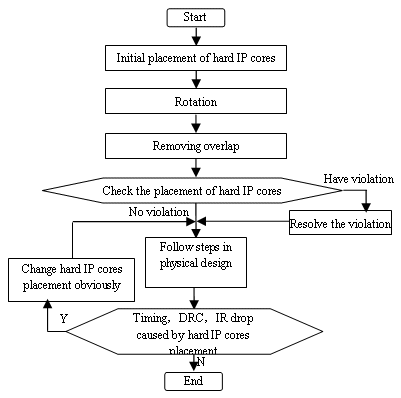
Figure 1. The hard IP core placement method
This hard IP core placement method is a general method and the steps may change a little according to the shape and the pin location of the IP cores. The IP cores have two mainly shapes: square and rectangle. The rotations of the rectangle IP cores may cause overlap, while the rotations of the square IP cores are not. Furthermore, the pins of the hard IP cores located differently, such as in corner, in one side and in two sides. The manual adjustment steps are presented as follows.
2.1 Rotation
The initial automatically placed hard IP cores need be rotated on condition that described as follows. Firstly, rotating the hard IP cores by users according to the locations of pins could reduce the wire length between the IP cores themselves. Secondly, the location of pins also have a directly relationship with the connection of relative standard cells. Rotation could reduce the congestion, improve the routability between hard IP cores and standard cells, and avoid the DRC violations such as spacing and short. However, the requirement of this rotation only can be obtained after the standard cells are placed or the route is finished. For a complex design, the rotation should get a tradeoff between all these factors mentioned above. Furthermore, the power grid will be cut off when encounters the hard IP cores, these modules should be rotated, if these IP cores are rectangle, to decrease or avoid the influence on power routing.
The 90°or 270° rotation of hard IP cores may cause overlap of the halo or themselves, if the IP cores are rectangle and the distances between them are not large enough. The overlap should be resolved later.
2.2 Removing overlap
Removing overlap is the next step in this method. Most of the overlap present to halo, which is popular and useful in current VLSI design. Halo, the area that prevents the placement of the standard cells within, is added around the hard IP cores in order to provide additional routing space and reduce congestion. The number of the halo is estimated according to the design itself, and the width of halo in the four sides may different. However, the halo is not taken into consideration in placement algorithm, which results in the overlap of hard IP cores are avoided whereas the halo may overlap. Furthermore, the rotation may cause overlap of the halo or cores themselves if the hard IP cores are not square.
The overlap of the hard IP cores will cause manufacture error, while the overlap of halo may cause placement error. And either overlap means the distance between the hard IP cores are too small to route or insert standard cells. The approach to remove the overlap is moving the hard IP cores which have the overlap to be separate manually as short as possible, while the general locations are changeless based on the initial placement.
2.3 Change the location obviously
When the slightly change steps are finished, the following steps in physical design will be implemented as typical physical design flow. Then, if there still have some timing violations, DRC violations or IR drop violations caused by the placement of some hard IP cores, change the location obviously step should be implemented. This step includes increase the distance of hard IP cores as long as need, exchange the location of several hard IP cores and move hard IP cores from one corner to another corner, according to the practical design. The distance of the hard IP cores could be estimated according to the target usage and the shape of the soft module, the number of hard IP cores that be placed inside this soft module, the shape and the pin locations of the hard IP cores, and the size of the soft module.
In practice, an obviously change of the location could resolve certain violations, but may cause the other violations because the complicated relationship of the design parameters. On this condition, this step need be done several times, in order to solve all the violations and get a tradeoff of the design parameters. The number of iteration depends on the design scale, design complexity, the number of hard IP cores, the requirement of the design parameters and the experience of the designers.
3. EXPERIMENTAL RESULTS
This method was implemented in a small test chip (chip 1) and an AVS HDTV decoder chip (chip 2). The RAM and ROM IP cores in these two chips, which are regarded as hard IP cores, should be pre-placed and placed inside the soft modules with certain area. What’s more, the IO cells are arranged and the locations of the soft modules are fixed before the hard IP cores are placed in chip 2. The design parameters of these two chips are listed in Table 1 and the manual adjustments of them are compared in Table 2. Furthermore, the application results of this method were compared with the automatic placement, which are shown in Figure 2 and Figure 3, and the relative data are listed in Table 3 and Table 4.
The AVS HDTV decoder chip has been delivered to the EDA center and under tape out now.
|
Chip 1 |
Chip 2 |
| Hard IP cores(number) |
10 |
126 |
| Soft module (number) |
1 |
15 |
| Standard cell (number) |
1000 |
40,000 in all |
| Hard IP core size |
varied |
varied |
| Hard IP core shape |
rectangle |
rectangle |
| Pins location |
4 in corner, 6 in left side |
all in both left side and right side |
| Halo |
four sides: 10um |
up, bottom: 10um left, right: 30um |
| Area |
5*5um^2 |
11000*11000um^2 |
| Library |
SMIC 180nm |
TSMC 90nm |
Table 1. The design parameters of two chips
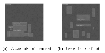
Figure 2. The compare hard IP core placement results of the test chip.
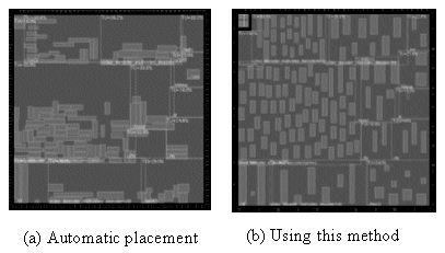
Figure 3. The compare results of the AVS HDTV decoder chip.
From these tables, we can get the conclusion that for these two different chips, the application of this method could obtain better results than the automatic placement in design parameters, such as timing, congestion, routability and IR drop.
4. CONCLUSION
A hard IP core placement method is proposed and used in designing a test chip and an AVS HDTV decoder chip. The designed results indicate that the proposed method is useful and helpful for complex VLSI physical design.
 Today, a lot of the system-on-chip (SoC) designs depend on Field-Programmable Gate Arrays (FPGAs) as a way to accelerate verification, early start of software development and validate the whole system before committing to silicon. This is done primarily to meet time-to-market demands. Today's FPGAs have the capability to contain a complex and large system-level design. However, in some cases, there is a requirement for these designs to be partitioned among several FPGAs for validation or prototyping. But, splitting the design into several FPGAs can create various partitioning issues, especially for relatively large designs with complex connectivity. These issues could possibly be circumvented if certain guidelines are followed. This paper talks about the general partitioning challenges and the guidelines that can be followed to get past these issues.
 Many argue that the focus point (and perhaps the linchpin) of successful supply chain management is inventories and inventory control. So how do food and agribusiness companies manage their inventories? What factors drive inventory costs? When might it make sense to keep larger inventories? Why were food companies quicker to pursue inventory reduction strategies than agribusiness firms?
 1 Abstract
 Implantable medical devices have been around for decades. Early on, most of the established applications for medical devices focused on cardiac rhythm management. Such devices were used to treat irregular heart rhythms, such as bradycardia (beating too slowly) or tachycardia (beating too fast).

 Digital circuits are circuits dealing with signals restricted to the extreme limits of zero and some full amount. This stands in contrast to analog circuits, in which signals are free to vary continuously between the limits imposed by power supply voltage and circuit resistances. These circuits find use in “true/false” logical operations and digital computation.
 Introduction
 The total does not include foundry sales.
 In many ways 2015 was a momentous year for the supply chain and logistics industry in terms of acquisitions and innovations.
  After 4 months of articles about data modeling, we're getting close to a functional database. I started this data modeling series with "Data Modeling" (April 2000), which discussed how to gather project requirements. I followed up with "Process Modeling" (May 2000), which reviewed process modeling and demonstrated my own variation of data-flow diagramming to illustrate what happens as data moves through the system. Then in "Entity Modeling" (June 2000), I developed a concept model, or entity relationship diagram (ERD), of the database. Last month, in "Logical Modeling" (July 2000), I translated that ERD into a logical model, which is a closer representation of the evolving database. This month, I develop a physical design that takes us one more step toward a working database.