Innovotek -News & BLOG

A blog about the news of the latest technology developments, breaking technology news, Innovotek Latest news and information tutorials on how to.

  • Home
    Home This is where you can find all the blog posts throughout the site.
  • Categories
    Categories Displays a list of categories from this blog.
  • Bloggers
    Bloggers Search for your favorite blogger from this site.
  • Login
    Login Login form

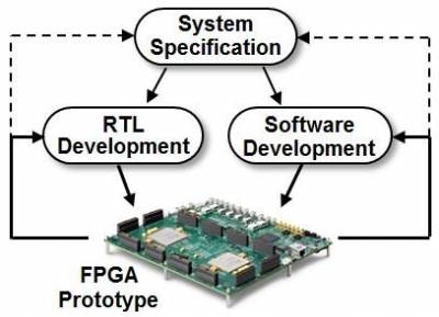
b2ap3_thumbnail_FPGA-Prototyping.jpgToday, a lot of the system-on-chip (SoC) designs depend on Field-Programmable Gate Arrays (FPGAs) as a way to accelerate verification, early start of software development and validate the whole system before committing to silicon. This is done primarily to meet time-to-market demands. Today's FPGAs have the capability to contain a complex and large system-level design. However, in some cases, there is a requirement for these designs to be partitioned among several FPGAs for validation or prototyping. But, splitting the design into several FPGAs can create various partitioning issues, especially for relatively large designs with complex connectivity. These issues could possibly be circumvented if certain guidelines are followed. This paper talks about the general partitioning challenges and the guidelines that can be followed to get past these issues.

Need For Partitioning:

As devices being prototyped on FPGAs are getting larger, following good design practices become important for all design flows. Adhering to recommended synchronous design practices makes designs more robust and easier to debug. Using an incremental compilation flow adds additional steps and requirements, but can provide significant benefits in design productivity by preserving the performance of critical blocks and reducing compilation time.

...
Hits: 47001
Rate this blog entry:
3

Posted by on in IC Design

b2ap3_thumbnail_AAEAAQAAAAAAAAPSAAAAJDJhZGFjZTUyLTZhYmItNDFiNC1hZGU1LWFlODRjZmRiODI5YQ.jpgImplantable medical devices have been around for decades. Early on, most of the established applications for medical devices focused on cardiac rhythm management. Such devices were used to treat irregular heart rhythms, such as bradycardia (beating too slowly) or tachycardia (beating too fast).

Alternatively, today’s implantable circuits provide therapy to treat numerous conditions. New applications in neurological stimulation can be used to treat sleep apnea, pain management, Parkinson’s disease, epilepsy, bladder control, gastrointestinal disorders, numerous autoimmune diseases, and psychological disorders, such as obsessive compulsive disorder (OCD). Meanwhile, implantable systems can now provide precise dosage and interval delivery of drugs to treat patients while minimizing side effects.

With the ever-increasing clinical need for implantable devices comes the continuous flow of technical challenges. As with commercial portable products, implantable devices share the same need to reduce size, weight, and power (SWaP). Thus, the need for device integration becomes imperative. There are many challenges when creating an implantable medical device.

...
Hits: 9816
Rate this blog entry:
2
joel-spolsky.jpg
 
Joel Spolsky: "The three things I would tell people to learn are economics, writing and C programming."
Image: Stack Exchange

For new programmers, knowing which languages and skills to learn can be overwhelming.

Just to secure a job interview, developers often have to show they are familiar with the long list of languages and associated technical skills demanded by employers.

While it can be tempting for new developers to dive straight into learning every skill recruiters ask for, those who want to maximise their chances of a successful career would be better served by first getting to grips with three fundamentals, according to Joel Spolsky.

...
Hits: 8734
Rate this blog entry:
2

In most cases today, IC power analysis efforts are mainly focused at signoff. Even though some place and route (P&R) solutions provide simple checks at the floor planning stage, there are a lot of opportunities to improve power analysis capabilities during design, and to align and integrate these with the signoff tools and the overall design flow. 


Figure 1. A full-flow approach to power analysis during IC physical
design.
 

Although every semiconductor company handles power analysis slightly differently, Figure 1 shows an idealized approach in which power analysis is embedded across the entire IC physical design flow. IC designers get their specifications from a cross-functional architecture power constraints definition, which is often called the “power budget.” This budget, which typically is fixed before any new IC implementation is started, specifies the maximum power permitted for the system, the board and the IC packages. At this point, the budget is essentially a rough estimate based on the know-how and experience of the IC, package and board engineers involved in the requirements definition for each new product development project. Once a high level budget is defined, it can be used to project the expected current flow and a power grid (PG) definition can be derived and partitioned into more detailed domains within the IC. The power grid should be able to accommodate the maximum expected current flows without a significant voltage drop given a design margin of around 10%. This sets the constraints for IC physical design implementation in a conventional P&R flow, which ends in a final power signoff analysis that validates the design against the power budget. Unfortunately, the process does not always proceed in this idealized, linear fashion. When the budget estimates are off, or the implementation is more difficult and power hungry than anticipated, “making ends meet” can become painful and lengthy.  This article describes in more detail how power constraints are enforced in the design flow and highlights areas of opportunity to improve the results, eliminating surprises, with a more robust power analysis capability.

Signoff Power Analysis

...
Hits: 10812
Rate this blog entry:
4

Posted by on in ASIC Design

Today, ASIC design flow is a very solid and mature process. The overall ASIC design flow and the various steps within the ASIC design flow have proven to be both practical and robust in multi-millions ASIC designs until now.

Each and every step of the ASIC design flow has a dedicated EDA tool that covers all the aspects related to the specific task perfectly. And most importantly, all the EDA tools can import and export the different file types to help making a flexible ASIC design flow that uses multiple tools from different vendors.

ASIC design flow is not exactly a push button process. To succeed in the ASIC design flow process, one must have: a robust and silicon-proven flow, a good understanding of the chip specifications and constraints, and an absolute domination over the required EDA tools (and their reports!).

...
Hits: 7953
Rate this blog entry:
3

Latest Article

General Partitioning Guidelines for Validation of Large ASIC Designs On FPGA
Today, a lot of the system-on-chip (SoC) designs depend on Field-...
Continue Reading...

Mailing List

sign up for email updates. We will make sure you are the first to hear Legal news .