Innovotek -News & BLOG
A blog about the news of the latest technology developments, breaking technology news, Innovotek Latest news and information tutorials on how to.
Efficient Verification and Virtual Prototyping of Analog and Mixed-Signal IP and SOCs Using Behavioral Models
- Font size: Larger Smaller
- Hits: 8930
- 0 Comments
- Subscribe to this entry
- Bookmark
 This paper describes the use of behavioral models and mixed-signal simulation as a means to verify the proper instantiation, connectivity and control of analog and mixed-signal (AMS) intellectual property (IP), and also as a means to prototype an AMS integrated circuit (IC) or system-on-chip (SOC) using behavioral models in place of IP modules yet to be designed. The goal of the first model use-case is to reduce the likelihood of human error resulting in IC functional faults. The goal of the second use-case is to develop an executable specification upon which the detailed design of IP blocks may be based.
1. Introduction:
As the size and complexity of SOCs and ICs increases, the critical task of finding and eliminating human error becomes more and more difficult – even for digital-only chips. Adding analog circuitry magnifies the problem. By its very nature, analog design and verification is more complicated than digital. When the design of analog modules is outsourced, the experience can be frustrating and traumatic enough for the faint-of-heart to avoid future purchases of analog IP altogether.
1.1 Analog and Mixed-Signal IP
Some have claimed that the term “Analog IP” is an oxymoron – that providing analog circuitry in a form which can be plugged in without analysis, and adjustment is simply impossible for other than trivial analog functions. [1]
The position of the article referenced above is that using IP should be as easy as attaching a new printer to your PC. And if the delivered package requires further customization for its end application whether by the vendor or customer, it is not properly IP at all. The vendor is providing a design service.
1.2 Difficulties of Reusing Analog/M-S IP
The design flow for analog systems is not as clean as is digital system design flow. Analog design flow cannot be automated; practical circuits can’t be automatically synthesized or optimized, mostly due to the fact that analog circuit design must address many more parameters than digital design. Furthermore, analog designs in general are not portable from one technology node to another. A change in technology involves at least device resizing and often requires architecture changes. In addition, once the analog IP is ready to deliver, its successful instantiation into the target circuit is prone to human error. Each bias and reference line requires correct electrical connection. Digital controls, clocks and data must be connected and the timing interface to the analog IP must be correct. [2]
1.3 Typical Attempted Solutions
In a typical approach the analog IP provider exhaustively simulates the IP using SPICE or an equivalent circuit simulator, and provides installation specifications and requirements documentation. It is then up to the buyer to ensure correct instantiation. When the IP buyers’ best efforts fail (or they decide to reduce their risk of failure) the IP provider becomes a design service provider playing a larger role in designing the IP into the SOC. A better approach is for the IP provider to supply a behavioral model along with the documentation so the buyers can reassure themselves by seeing the IP operate in their verification environment. Questions arise regarding the quality of the behavioral models. In many cases for the sake of simplicity, execution speed, and quickly getting the verification platform up and running, the models do not accurately incorporate the functionality of every port in the IP cell. In the worst case, too simple a model can camouflage mistakes in its instantiation or control.
1.4 Efficient Use of Behavioral Models
An inaccurate model is worse than no model at all. Falsely reporting failures can delay final tape-out or cause unnecessary redesign of the target SOC. Worse than that, false optimism may allow design bugs to escape into Silicon, possibly wasting millions of dollars and months of redesign. It’s difficult to argue against model accuracy, but what about simulation time? A totally accurate PLL model may be required to verify certain functionalities, but requires mille-seconds to start up, acquire and lock. Running hundreds of regression simulations with such long run times is obviously unacceptable. The solution this paper proposes is to use multiple model views, targeted toward executing each testcase of the verification plan with no more than adequate accuracy.
1.5 Overview of Following Sections
The remainder of this paper discusses the following topics. Section 2 describes the concept of using multiple model styles or views, and choosing from the collection of styles to optimize speed versus required accuracy for efficient simulations. Section 3 discusses the use of behavioral models to prototype an SOC, describing a top-down design methodology, using behavioral models as an executable specification when designing or purchasing analog IP and using behavioral models to enable reuse of existing analog IP. Section 4 deals with efficient verification of mixed signal SOCs, from developing a verification plan (V-Plan), to creating testcases, to choosing model views for each testcase. A partial V-plan is developed for a hypothetical SOC, and model view choices made for several testcases. Section 5 talks about two approaches managing the various model views and how the choice of one view over another is made at simulation run time, whether manually or as part of a regression script. Conclusions are summarized in section 6.
2. Multiple, Targeted Model Views
Fundamentally there is a trade-off between model accuracy and model execution speed. The next paragraphs talk about various model levels and their appropriate use.
2.1 Fully Electrical
These have the highest level of detail but slowest execution. May be written in Verilog-A, Verilog-AMS or VHDL-AMS, the fully electrical model view is compatible with device-level netlists (transistors). Verilog-A models are executable in SPICE-like simulation environments such as Spectre, H-Spice and Eldo. All Verilog-A I/O and internal nodes must be electrical in nature, even those of digital functionality. Verilog-AMS and VHDL-AMS may only be run in AMS simulators such as Cadence’s AMS Designer and Mentor’s Advance AMS. Fully Electrical models are the most detailed and exhibit conservation of charge on all electrical I/O and internal nodes. (The AMS languages include the possibility of digital I/O and internal nodes which are described behaviorally). The circuit is described in terms of voltage and current flow. Generally unsuitable for SOC verification, fully electrical models are valuable in top-down design flows and in verification of analog sub-systems.
2.2 Behavioral Electrical
These have less detail but execute faster than fully electrical models. Written in Verilog-AMS or VHDL-AMS, these models describe analog behavior in terms of algebraic and differential equations rather than voltage and current. Their electrical I/O exhibit conservation of charge but internal functional behavior is described by real variables wherever possible. Behavior may be as accurate as required by skewing the modeling style toward the Fully Electrical behavior. This level of model is the most suitable for detailed SOC verification of the interface, timing and control of the collection of analog IP blocks in their entirety.
2.3 Signal Flow, with or without Electrical Behavior
These have less detail than the two preceding styles and execute much faster. This model style may be written in plain digital VHDL or in Verilog-AMS. The signal path through the model avoids the use of an analog circuit solver. It combines event-driven and self-timed analysis and executes simple mathematical processing of the signal. Verilog-AMS and VHDL-AMS models can use this approach while simultaneously using an electrical approach to monitor bias currents and reference voltages. Plain VHDL (without electrical behavior) can use the signal flow approach without requiring the AMS language extension. Plain digital Verilog has no concept of real wires or ports, but Verilog-AMS includes ports and wires of type wreal (for wire-real). There is no feedback path in this style of modeling, and there is no analog solver to choose the sampling points. Op-amps along with their feedback network are replaced by gain blocks. A built in sampling plan must be written into the model which obeys the Nyquist criteria. As one might expect, this style of model executes blazingly fast and is the top choice for verifying the full SOC signal path including the analog section. Modeling the signal path using reals (or wreals) and using electrical modeling techniques for the bias and reference network, results in a nice combination of verification coverage and high execution speed.
2.4 Plain Digital Equivalent
Written in plain digital Verilog, these are the fastest of all Verilog models. Since Verilog doesn’t allow real nets or ports, a rather tedious but rewarding workaround uses out-of-module references (OOMRs) to pass signals from one digitally-modeled analog block to the next all the way from the input source to the A/D converter. It must be assumed that connectivity and bias integrity are verified in other testcases using more accurate models. This model type is suitable for simulating an extensive digital section of the SOC along with the analog front end.
2.5 Base-band Equivalent Models for RF
Verifying an SOC’s instantiation of RF IP blocks should not require verifying the RF IP itself. That is best left to specialized RF simulators. As in the PLL example, a very few testcases may require accurate wide-band models of the RF IP blocks. For the bulk of full chip verification it is often acceptable to use base-band equivalent models. In these models of the PLL, Signal Source, LNA, Filter and Mixer, the positive/negative paths are replaced by I/Q paths. A frequency variable is passed by OOMR from the behavioral PLL model to the other RF blocks. The models are written to verify the correct PLL frequency and correct biasing and control but execute much faster than wide band models which would be required to operate at greater than twice the carrier frequency.
3. Prototyping with AMS Models
Ken Kundert points out “The key to improve analog design productivity and efficiency lies in the ability of the design organization to be able to develop and deploy a ‘systematic design methodology’, not in tool automation alone.” [3] This section describes a prototyping methodology using behavioral models which then act as an executable specification for the analog IP to be developed.
3.1 Mixed-signal Methodology
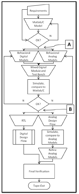
Figure 1 shows the flow chart of a top-down mixed-signal design methodology incorporating a prototyping phase using behavioral models of intellectual property yet to be designed. The prototyping phase begins at the point marked “A” and ends at point “B”. At “A”, an architectural-level model has been created using Matlab, the C language or some other high level modeling language and simulation tool, and accepted by manually inspecting and comparing to requirements. It is then a manual task to translate the high-level model into digital and analog behavioral models and integrate them into a top-level module and test bench. This test bench must be simulated and its behavior manually compared to that of the architectural level model.
As to the choice of model styles to use in the prototyping stage, begin with the all-digital equivalent described in 2.4. Compare the behavior to that of the architectural-level simulation, and then evolve the model into the signal flow type described in 2.3. Once accepted (at point “B”), the model prototypes evolve further to become executable design specifications.

Figure 1: Top-Down Mixed-Signal Design Flow
Unlike the manual comparison between the prototype and the architectural level simulation, from point “B” forward the “real” design can be substituted and simulated in whole or in part for the prototype behavioral models. From point “B” there is a well known and mature design and verification flow for the modules comprising the digital portion of the IC.
For top-down analog module design flow, each behavioral model used in the prototyping phase is instantiated into its own testbench along with a stimulus driver and stimuli waveforms created to generate all the required analog behavior. Fully electrical models using Verilog-A as described in section 2.1 or behavioral electrical models as in section 2.2 are provided to the analog design team. Detailed analog design may continue and AMS simulations run on platforms such as Cadence’s Analog Design Environment (ADE) or Mentor Graphics’ Advance AMS.
This package serves for both specification and model validation. The initial model versions might only include signal I/O and control. The transistor-level design will require power supplies, reference voltages and bias currents. As these are added to the schematic and symbol, the model and the stimulus driver are revised to include the actual pin-out. The model behavior is refined to match the circuit’s behavior. As the analog block design is completed, and the final refinements are made to the model, the top-level testbench is also modified to fit the final analog block. The final full-chip behavior must again be verified versus the accepted architectural-level behavior.
Successful functional verification is the final step before tape-out and is discussed in section 4.
3.2 IP Purchase and Reuse
Two important use cases are the purchase and reuse of IP. The behavioral model prototypes once accepted at point “B” and packaged with a testbench and set of stimuli as described above may become part of the requirements document when purchasing digital or analog IP from a vendor. Conversely, when one has IP on hand from a previous project using this flow, use its behavioral models in the prototyping phase.
4. Verification with AMS Models:
The starting point for efficient verification is the Specification Document, from which a Verification Plan Document (V-Plan) is developed. The V-Plan includes a list of testcases which when successfully executed verifies all of the device specifications are properly designed. Each test case implies a certain degree of model accuracy on the part of the models of the analog IP.
4.1 Specific Example
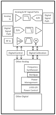
Figure 2 is an iconic diagram of an RF mixed signal SOC showing
- Analog-to-digital, digital-to-analog and RF down-conversion paths
- Other analog functional blocks
- Digital modules to calibrate and control the analog functional blocks
- Other digital functional blocks

Figure 2: A Mixed-Signal SOC Diagram
Some of the testcase categories for a representative V-plan appear in Table 1.
![]()
Table 1: Partial V-Plan Categories
Taking a PLL model as an example, one or a few testcases in the Calibration or Control categories might require a Behavioral Electrical view which exhibits detailed and accurate (but slow-executing) analog behavior such as frequency acquisition and phase lock. A few testcases in the Signal Variants category may require less detail, possibly a model which exhibits an idealized transition between frequencies. A Signal Flow model would be an adequate choice. Maybe 99% of the SOC testcases do not focus on the PLL at all. For most Signal Variants and all Digital Functional testcases a Plain Digital Equivalent is the fastest choice and is perfectly adequate.
The bottom line requirement is to fulfill the Verification Plan as efficiently as possible. If highly accurate models are used in all testcases, regression simulations will require an unacceptably long time. Not enough accuracy will result in coverage holes and risk of faulty Silicon. Choosing from a variety of model views can cover the entire V-Plan in a patchwork manner in a reasonable amount of time.
5. Managing Model Views
The case for requiring several model view types has been presented, but how are the view types chosen and compiled into the simulation database? Two methods exist.
`ifdef Beh_Elec
//… Beh_Elec Model Code
`elseif Sig_Flow
//… Sig_Flow Model Code
`else
//… Dig_Eq Model Code
`endif
6. Summary and Conclusions:
This paper presented the case for requiring and using multiple model views or styles of analog behavioral models, and how to take advantage of each style of model to improve the quality and efficiency of SOC prototyping and verification. Taking the time to set up a top-down design methodology followed by a well-planned bottom-up verification methodology can improve the chances of first-time Silicon success and faster time to market.
