Innovotek -News & BLOG

A blog about the news of the latest technology developments, breaking technology news, Innovotek Latest news and information tutorials on how to.

  • Home
    Home This is where you can find all the blog posts throughout the site.
  • Categories
    Categories Displays a list of categories from this blog.
  • Bloggers
    Bloggers Search for your favorite blogger from this site.
  • Login
    Login Login form
Recent blog posts

b2ap3_thumbnail_cedronics-physical-design-250x250.gifWhen designing a product that operates off of a small battery, low power consumption is extremely critical. A well-designed power system can be a key differentiator for a competitive low-power product. Designing an ultra-low-power system, on the other hand, can be a highly complex undertaking. A design team needs to balance and integrate a variety of low-power design approaches and techniques to achieve their goals. Using a combination of multiple power domains and operating voltages, along with thorough statistical analysis, a low power product can be designed to provide a competitive advantage.

Any company that develops products that operate off a small battery can benefit from considering well-integrated, physical design practices for low power consumption design targets. Wireless sensors, mesh networks, wearables, Bluetooth devices, Internet of Thing (IoT) devices, hearing aids, mobile phone audio/video processing capabilities, tablets and headsets all require an optimized approach to achieve ultra-low power.

So, what is it that these ultra-low-power products need? Often, a minimum clock rate will be used meet performance goals. Higher threshold voltage (VT) devices may be used to minimize leakage. Perhaps multiple clock domains, multiple power domains and/or multiple operating voltages will be part of the low-power design solution. Lower operating and standby voltages lead to much lower overall power consumption; however, multiple power domains also result in a complex SOC (system on a chip) power structure.

...
Hits: 5676
Rate this blog entry:
2

b2ap3_thumbnail_download.pngAbstract
Simulink models are used as executable specifications in commonly used design flows for mixed-signal ASICs. Based on these specifications, analog and digital components are directly implemented in mixed-signal design environments. This step constitutes a large leap of abstraction. In this work, we address this aspect by showing and discussing an approach for automated transitions from Simulink models representing analog and digital components to HDL descriptions using HDL Coder. On the one hand, we translate analog Simulink components into continuous-value discrete-time HDL descriptions that can serve as reference behavioral models in the mixed-signal design environment. On the other hand, for digital Simulink components, we developed optimizations for Simulink models in order to achieve resource-efficient HDL descriptions. Both solutions in the analog and digital domain were integrated into Simulink Model Advisor. An evaluation of the presented design flow, as applied to an automotive hardware design, is shown.

Introduction
Electronic Control Units (ECUs) in the field of automotive electronics generally interact with the physical environment by using sensors and actuators. Thereby, mixed-signal ASICs (Application Specific Integrated Circuits) are needed as an interface between microcontrollers and sensors as well as actuators. In this work, we focus on ASICs connected to sensors, whereby the sensor is often enclosed with the ASIC into a system-in-package (SiP). In the most general case, mixed-signal ASICs consist of analog, non-programmable digital and programmable digital components.

The increasing integration density of ASICs allows more and more functionality, which leads to more complex ASIC designs. These require a holistic view on a high abstraction level at the beginning of the design. Therefore, a system-level (SL) design methodology is needed, where all ASIC components and the associated sensor are modeled in a common SL design environment. In standard flows, the design starts by developing an SL model that serves as executable functional specification. Based on this specification, the particular ASIC components are designed on implementation level (IL) isolated from the overall system and without any reuse of the design effort performed at SL. The isolation between SL and IL constitutes a gap in the design flow, which leads to redundant implementation efforts and consistency problems between SL and IL. Furthermore, the isolation of components from the overall system during implementation leads to lost optimization potential. That is why in (1), we proposed a seamless SL design methodology, which uses automated transitions from SL to IL models in order to reduce the effort of design transfer between SL and IL (see Figure 1).

...
Hits: 5398
Rate this blog entry:
2

b2ap3_thumbnail_IC31.gif

Abstract:
This paper aims to emphasize on the importance of integrating design for failure analysis in the layout considerations during the IC development process. It will have a brief overview on the importance of failure analysis in an IC development process, followed by an understanding of the failure analysis methodologies in the industries. This leads us to the different considerations in the layout of ICs to facilitate failure analysis, and also the challenges in failure analysis with increasing complexities when the design approaches nano-electronics.


I. INTRODUCTION

The introduction of the System-on-a-Chip (SOC) and the increasing complexity of ASIC designs has made testability and analysis of Integrated Circuits (IC) more challenging. It has almost become a mandatory requirement to do a Design-for-Testability (DFT) and Design-for-Analysis (DFA) before the freezing of the ASIC design as the ability to test and analyze a complex design will bring about a shorter product cycle and faster time-to-market. In DFT, testability requirements are presented in various levels of an SOC. In terms of failure analysis, there are many techniques available to analyze the device for physical defects, from isolate the faulty behavior to the failing transistor and to capture the images at localized root cause in substrate level to understand the failing root cause. Unfortunately, even though there are many existing techniques available for failure analysis, the analysis may not always be possible. This is because the inevitable trend in IC design is that most of the time, in order to have a faster time to market, IC designers need to embed cores that are untested and are not manufactured in-house. There are inadequate considerations in the IC layout that make analyzability of an IC difficult or impossible. Furthermore, smaller technology nodes also brings about an increase in the metal layers of an IC, new materials in wafer manufacturing processes and different IC packages which pose greater challenges to failure analysis. These challenges lead to higher equipment cost, more experienced manpower required, longer analysis turn around time and difficulties in the analyzability of an IC. Even for reused IP which are proven in the design, process shrinking or backend process parameters shift may bring problems like higher leakage current and reduced reliability. Hence there is an increasing need to integrate failure analysis requirements with the IC development in an early phase. Strong interactions between development team and failure analysts are required to identify the possible bottlenecks from the very beginning and provide solutions with adequate layout considerations. 

II. FAILURE ANALYSIS – THE DIFFERENT METHODOLOGIES

Failure analysis for integrated circuits is increasingly important and very much required for today’s complicated packaging and technology strategies. It is a process which requires the combination of analysis experiences, leading-edge equipment and techniques, and well defined failure analysis procedures to achieve fast turn around time for failure root cause findings. Failure analysis methodologies are important to the IC development process as it allows one to effectively identify the root cause of a design or process bug. The challenge of making rapid improvements in IC design and technology also requires the development of relevant failure analysis techniques. There are many analysis techniques and they can be generally divided into the 3 areas:

1. Chemical or physical preparation of the integrated circuits.
2. Fault localization of integrated circuit’s failing behavior.
3. Fault imaging of integrated circuits.

Chemical or physical preparation of the integrated circuit is the first step in the analysis of failing devices. The package has to be opened up either on the front or backside so as to allow further localization techniques to be carried out. Improved packaging techniques like Ball Grid Array (BGA) packaging had make the chemical or physical preparation increasingly challenging for failure analysis. This is an important process whereby one has to be careful not to destroy the failing signature and the electrical functions of a device.

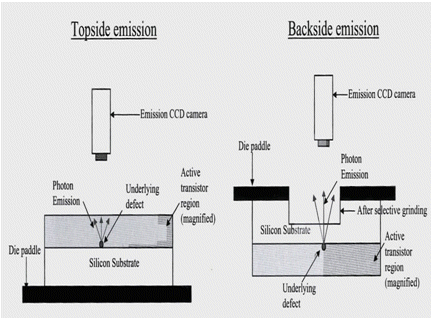
Fault localization is the process where various techniques are used to isolate the defective areas on the die. Techniques like photoemission microscopy uses faint Infra-red radiation emitted by leakage current to localize the leakage site. Other techniques such as Thermal Induce Voltage Alteration (TIVA) uses the active approach whereby failure sites are located use a scanning ionizing beam, such as laser beams, to stimulate failures that are sensitive to carrier generation or thermal stimulation.[1] This allows one to reduce the area required for analysis and significantly save on the time required for failure analysis. The localized defect is then characterized with a view to understand the failure mechanism.


Fig. 1. Top and bottom photoemission setup in fault localization

The final step of failure analysis after fault localization is fault imaging. Failure analysis can only be completed once the root cause of the failure has been identified. Hence the defect must be imaged to prove the defective behavior. Optical microscopy is the obvious and most basic equipment for this purpose. However, with the complexity of microelectronics today, optical microscopy is of limited use. In order to achieve better resolution for imaging, microscopy is available using all kinds of beams: ultrasonic, electromagnetic (from infrared to x-ray) and particles like electrons and ions or near-field interactions with a stylus, as in scanning probe microscopy. All these imaging tools are equipped with CAD layout information for better navigation over the die. The FA processes can be generally summarized in the following table


...
Hits: 6128
Rate this blog entry:
2

Posted by on in IC Design

offering a custom silicon and software intended to streamline the design process for e-books using the same E-Ink display. 

TI's chips and software also are intended to allow OEMs to lengthen the battery lifetime of their e-books by 50 percent while shrinking the footprint by eliminating 40 discrete components.

"We are offering a comprehensive e-book development platform to e-book developers that will speed their time to market, lower their BOM, shrink their footprint by 200 square millimeters and increase their battery lifetime by about 50 percent," claimed Gregg Burke, TI's eBook business line manager.

...
Hits: 5332
Rate this blog entry:
2

Latest Article

General Partitioning Guidelines for Validation of Large ASIC Designs On FPGA
Today, a lot of the system-on-chip (SoC) designs depend on Field-...
Continue Reading...

Mailing List

sign up for email updates. We will make sure you are the first to hear Legal news .