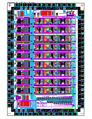
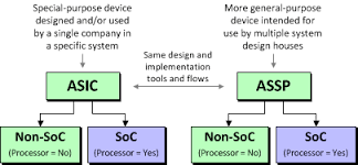
 Application specific integrated circuits (ASICs) typically conjure up the notion of massively complex logic chips containing tens or hundreds of thousands (even millions) of transistors configured to solve a customer’s unique set of problems. Unlike multi-function standard product ICs such as a micro-controller that can find its way into a wide variety of applications, ASICs are designed for one specific application and generally for one specific product or product family.To better understand the role and applicability of ASICs, it is important to briefly review their historical origins.
The first integrated circuits from the early ‘60s contained just a few transistors and performed simple digital logic functions such as "and", "or", "nor", etc. These were called SSI devices, meaning small-scale integration. As photolithography techniques improved, more and more transistors could be built on a single sliver of silicon. Soon, chip companies were developing medium scale integration (MSI) functions like flip-flops, buffers, latches, etc (10-100 transistors). Large-scale integration or LSI (100-1,000 transistors) and eventually VLSI (up to 100,000 transistors) ICs followed, providing lower system costs and higher levels of performance. Today, of course, we have digital chips in excess of a billion transistors thanks to advanced sub-micron lithography and the low voltage, high speed processes upon which they are built.
The first digital ASICs were built using a standard cell library consisting of fixed-height, variable-width ‘tiles’ containing the digital logic functions discussed above. The ability to reuse these blocks over and over saved time and money when designing a custom logic IC. Analog ICs were initially comprised of a pair of matched transistors and soon expanded to include rudimentary op amps, voltage regulators, comparators, timers and much more.
Demands of analog
Analog applications typically involve much higher voltages, so these ICs needed their own unique set of manufacturing processes. More recently, market demands for smaller size, higher speeds and lower power consumption have forced a merging of analog and digital functionality on a single silicon chip. Cells consisting of the basic analog building blocks discussed above were created and added to the digital libraries. These Analog cells were restricted to the digital fab processes developed for predominately logic applications.
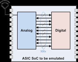
Today, most ASIC companies offer some degree of analog functionality as a part of their services. In many cases, the analog functions are mimicked with digital design techniques. In others, compromises to the analog functionality must be made to facilitate the use of standard library cells that are designed to yield well in the fab processes developed for high speed, high density, low power digital designs. Often, these chips are referred to as Mixed-signal ASICs or as big “D”, little “A” ASICs, meaning high digital content and minimal analog content.
Analog ASICs play a critical role in our lives. Without them, none of the portable electronic devices we use in our daily lives would exist. Imagine a world without cell phones, MP3 players and navigation systems. Building them with standard products would make them prohibitively expensive and physically impossible to carry in our purses or pockets. Every automobile contains dozens of ASIC chips for everything from climate control to airbag deployment; suspension control to entertainment systems. ASICs also play important roles in applications for hospital medical equipment, eMeters, home appliances such as washers and dryers, scuba gear, hearing aids, and much more.
Picking an ASIC design partner
The analog ASIC market is huge. In fact, research firm IC Insights reports that almost 60% of the nearly $37B of analog ICs sold in 2010 were ASICs. Yet very few mixed-signal ASIC design houses fully understand the implications of custom analog design and its applicability to analog-centric ASICs. ASICs requiring high analog content should be directed to those design houses that specialize in analog circuit design rather than those who simply select analog IP blocks from a library. Analog ASIC companies have large staffs of competent, experienced, analog engineers with expertise in a wide range of analog functions.
Reviewing an ASIC house’s patent portfolio as a quick guide as to the creativity of its engineering team will serve as a first order measure of its analog expertise.
Clearly, the large analog IC houses (like ADI, Linear Tech, Maxim, National, TI) have patent portfolios a mile deep. Those that also engage in analog ASIC development set high bars regarding who can access this capability and impose high minimum order requirements. For example, TI reports that their application-specific analog business focuses on a small number of large customers like Seagate, Sony, Samsung, Hitachi Global Storage Technology, Toshiba and a few others that require custom application-specific products. Minimum annual unit and or dollar volumes force the majority of the smaller customers to seek out independent analog or mixed-signal ASIC design houses.
 These days, a typical corner (TT) is no longer typical for most applications. For that matter, standard PVT Corners (FF/TT/SS), generally, do not represent the exact environmental conditions in which an ASIC/SoC will be functioning. This means the voltage may not be a nominal Vdd in a typical case or Vdd±10% in an extreme case; and the temperature may not be 25C in a typical case or 125C/-40C in extreme cases. Also, in today's market, everyµW of power saved, and nS of delay avoided, makes a significant difference in a product's performance and cost. Therefore, it is important to know how a system behaves under real-time PVT conditions. One needs to characterise foundation IPs at these special (custom) corners to avoid overdesign and achieve optimal product for best power and performance. When estimating the power and timing numbers of an IP at a custom corner (e.g., @95C and Vdd+3%), it is not easy to derive values from regular SS, TT, and FF characteristics as these may not support linear extrapolations. Even small errors in calculation can be very risky. One approach is to use characterisation tools (e.g., Silicon Smart from Synopsys) that can easily characterise foundation IPs to estimate power and performance of an SoC at any custom corner with substantial accuracy using reference ".lib" files.
 Chip design costs are expected to shoot up, but
  What if the supply chain community could emulate the “Internet world” and create a universal, open logistics network that is economically, environmentally, and socially efficient and sustainable? Such a concept exists, and it’s called the Physical Internet. Today the Physical Internet is a vision for an end-to-end global logistic network, but there are plans to turn it into a reality by 2050.
 Application specific integrated circuits (ASICs) typically conjure up the notion of massively complex logic chips containing tens or hundreds of thousands (even millions) of transistors configured to solve a customer’s unique set of problems. Unlike multi-function standard product ICs such as a micro-controller that can find its way into a wide variety of applications, ASICs are designed for one specific application and generally for one specific product or product family.To better understand the role and applicability of ASICs, it is important to briefly review their historical origins.
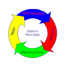 Following a series of fatal accidents in the mid-1990s, a formal investigation was conducted with the Therac-25 radiotherapy machine. Led by Nancy Leveson of the University of Washington, the investigation resulted in a set of recommendations on how to create safety-critical software solutions in an objective manner. Since then, industries as disparate as aerospace, automotive and industrial control have encapsulated the practices and processes for creating safety- and/or security-critical systems in an objective manner into industry standards.
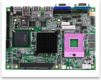 When designing a product that operates off of a small battery, low power consumption is extremely critical. A well-designed power system can be a key differentiator for a competitive low-power product. Designing an ultra-low-power system, on the other hand, can be a highly complex undertaking. A design team needs to balance and integrate a variety of low-power design approaches and techniques to achieve their goals. Using a combination of multiple power domains and operating voltages, along with thorough statistical analysis, a low power product can be designed to provide a competitive advantage.
 Abstract