 Abstract:
This paper will explain how new ASSP ventures face challenges that can derail success of a product even before the first device is sold, including market entry barriers such as time to market pressures, limited human and financial resources, and increased design complexity. In order to overcome these hurdles, these companies must consider a business model that enables a cost-effective design methodology flexible enough to allow changes within this unstable market environment. ASSP prototyping with FPGAs and then migrating to structured ASICs for production provides the best answer to this critical dilemma.
Introduction
System companies looking to implement new ideas in integrated circuits are faced with several challenges today, including higher upfront costs, increased risk due to higher design complexity and shrinking market windows. Traditional technology choices have included cell-based application specific integrated circuits (ASICs), application specific standard products (ASSPs), field programmable gate arrays (FPGAs) or microprocessors and digital signal processors (DSPs). While each of these technologies has its own pros and cons, standard cell ASICs have historically been the best option in the production phase of a design providing the lowest unit production costs and lowest power consumption for system design.
However, designing a standard cell ASIC at the 90-nm node today is both an expensive and risky development proposition. Non-recurring engineering costs (NREs), including cost of mask-sets, and engineering design efforts such as layout and verification, continue to rise as designs migrate to manufacturing technologies using smaller process geometries. Total development costs of a single complex, high-density standard cell ASIC at the 90-nm process node, can be in the $20-30 million range (see Figure 1).
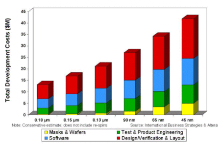
Figure 1. Increasing Development Costs
Getting a device functioning correctly the first time is imperative to avoid additional costs and delays associated with re-spinning the ASIC. Simulation, verification and validation of a design must be performed to ensure that the ASIC design is correct before tape-out and after silicon has been received. Re-spins pose serious problems, not only increasing costs of engineering and mask-sets but also from a lost market opportunity perspective. According to International Business Strategies, being 3 to 12 months late to market with a product can result in a potential sales loss ranging from 27 to 91 percent, respectively (see Table 1).
| Time-To-Market |
Potential Sales Achieved |
| First-To-Market |
100% |
| 3 Months Late |
73% |
| 6 Months Late |
53% |
| 9 Months Late |
32% |
| 12 Months Late |
9% |
Table 1. Time-to-market matters
These increased costs and high design risks are forcing designers to do a more thorough return on investment (ROI) analysis to justify these expenses, which usually demands significant unit volumes be shipped to ensure an acceptable return. For example, if a company spends 20 percent of its estimated revenue on research and development for a 90-nm, high-density standard cell ASIC, say $30 million, device revenue would have to hit $150 million per year. A single device rarely has more than a 10 percent market share, therefore a total market size of $1.5 billion would be needed to ensure an acceptable ROI.
The following example illustrates the magnitude of this volume requirement. Assuming a chip has an average selling price of $10, this device would need a run rate of 15 million units per year to generate $150 million in revenue. With the exception of highly popular digital consumer products such as MP3 players or certain gaming consoles, very few markets approach this size.
Design Alternatives Provide Lower-Risk and Smaller Upfront Costs
Historically, FPGAs have been perceived as cost prohibitive, and performance and density limited when compared to standard cell ASICs. However, FPGAs today are manufactured on leading edge 90-nm processes that have allowed them to meet a majority of new ASIC or ASSP design start requirements due to significant improvements in performance, density and cost. In fact, 80 percent of ASIC design starts are of a density that can be prototyped with a single high density FPGA. FPGAs built on 90-nm process technologies offer core performance in the hundreds of MHz range, I/O performance capabilities in the gigahertz range, gate densities in the millions of gates and costs ranging from under $10 per unit to nearly $1,000 per unit.
Using FPGAs for ASIC or ASSP prototyping and then migrating to structured ASICs for production can help reduce these development costs and mitigate design risks. Designers can use an FPGA to minimize upfront investment since FPGAs have zero NRE, perform in-system verification to fix design bugs, remove technical risk and demonstrate their technology to customers prior to device production. Designers can also get a head start on system development and qualification with customers in the field, thereby removing market risk while ensuring customer acceptance of the product. As demand for the end product increases, designers can then move seamlessly to a structured ASIC for a fast path to production (turnaround time in weeks) with upfront NRE costs that are a fraction of ASIC NREs. This development flow bypasses the pain and expense of traditional ASIC development while still meeting cost, performance and power requirements.
Case Study
New ASSP ventures face barriers to market entry including tighter venture funding, fragmented end markets and shrinking market windows. One such example is the communication group at Infineon Technologies. A smaller group within a large, multinational semiconductor manufacturing company, the Infineon communication group was designing the MetroMapper 622 ASSP chip, which is a mapper/framer capable of mapping datacom traffic into SONET/SDH transport payloads.
The Infineon group faced multiple challenges such as time to market pressures, limited engineering resources, limited funding for chip development and a set of customers each looking for customization of the ASSP device to better fit their end systems.
Unwilling or unable to risk losing millions of dollars over failed design starts using a standard cell ASIC, the Infineon group sought alternative solutions and elected to design with Altera Stratix FPGAs and HardCopy structured ASICs. The group was able to test the functionality of its design in the field within customer end systems prior to production. Prototyping with the Stratix FPGA enabled minor design modifications and debugging. After in-system validation, the Infineon design was migrated to the HardCopy structured ASIC by Altera’s design center.
The successful design migration was made possible by footprint compatible packages, equivalent logic element structures, clock networks, I/O buffers, PLLs, memory blocks and similar process technology in the Stratix FPGA and HardCopy structured ASIC. This unique design methodology ensured first-time design success with the HardCopy structured ASIC. It also minimized the upfront costs due to the zero NRE of the Stratix FPGAs and dramatically lower NRE for the HardCopy device compared to standard cell ASICs. Moreover, the flexibility of the FPGA allowed the Infineon group to uniquely customize the designs for its end customers while still getting its product to market early. The 10-week turnaround time for the HardCopy prototypes enabled the Infineon group to quickly ramp its products into production at device costs at a fraction of what the group paid for the FPGA.
One Infineon customer was concerned about protecting its IP from other users of the ASSP device and requested a custom structured ASIC. The Infineon group migrated the customer’s design to a distinct HardCopy device, thereby limiting its purchase and use to this customer. Infineon was able to capture market share based on meeting the customer’s need for customization using this unique, flexible and cost-effective FPGA to structured ASIC migration solution.
Advantages of FPGA Prototyping
This case study is just one example of the benefits of prototyping with an FPGA and then migrating the design to a structured ASIC. Whether a product is new or mature, these challenges also exist in other markets. It is important that design teams recognize these hurdles and choose a fiscally-sound design strategy that provides the flexibility to make changes as the market dictates.
FPGAs continue to evolve, narrowing the performance, density and cost gaps with ASICs and ASSPs. In addition, FPGA design flows are increasingly mimicking ASIC/ASSP design flows. These methodologies differ, however, in that proprietary FPGA design software offers some innovative technologies to speed system design and take advantage of the programmable nature of FPGAs for in-system verification.
Prototyping an ASIC or ASSP design using FPGAs can relieve the time bottleneck and remove the high-caliber compute resources required to functionally verify a sub-average to large-sized design. In addition, prototyping can provide other, more enticing, benefits. A single prototype, for example, can serve to verify hardware, firmware and application software design functionality before first silicon is brought in-house.
In the ASIC/ASSP development process, hardware developers are concerned about how they will integrate external IP they don’t fully understand. The IP can be hard or soft, with each type presenting different integration challenges. The need to develop derivatives must be accounted for in the original design—if not, developing a derivative can become as tough as developing a new product.
Software developers need to use real hardware during design work because simulation models can’t provide the speed they need—even when accelerated. Software developers want to use their familiar development and debug environments, not Verilog and a waveform viewer, to debug their code.
A FPGA-based prototype can address the needs of both hardware and software developers. Given low design stability, firmware and application software, developers usually request hardware design changes that require a re-configurable prototype. To enable that, the FPGA on the prototype must be re-programmable. SRAM-based FPGAs provide this capability. In addition, since the speed of the system must be high enough to enable fast OS booting and application software testing, high-performance FPGAs can do the trick with block speeds of more than 350 MHz and average system speeds of approximately 200 MHz.
To prevent intellectual property theft, the design has to be “secure” as FPGA-based prototypes are moved around from one geographic location to another. A high-density FPGA can incorporate a design security feature based on a 128-bit advanced encryption standard (AES) algorithm. The key is stored in a non-volatile location in the device itself, which remains reprogrammable with the key.
With large device pin-out counts and small pin spacings, successfully assigning physical pin numbers to ports of each FPGA design can be influenced by several factors, including routability of the FPGA, placement of the FPGA relative to its neighboring components on the PCB, system interface location constraints and PCB routability. Tools that provide pin assignment flexibility, available in proprietary FPGA design software, are critical to the pin planning process.
ASIC and ASSP hardware designers have an affinity for scripting. Their flows use and apply automation within a single tool flow and between multiple tools used in projects. Initially, as a design is compiled into a FPGA, designers may use graphical tools. However, as design iterations increase, the need to automate becomes paramount.
Proprietary FPGA design software provides tool command language (Tcl) scripts, allowing the designer to perform a wide range of functions, such as compiling a design or writing procedures to automate common tasks.
Medium to large scale designs will often require more than one person to design and implement the design blocks. Various teams working in different locations is the norm, especially with high-end ASIC design work. Either an entire FPGA or a portion of an FPGA should be dedicated to each team, providing a block-based design flow that enables design, optimization and locking down the design one block at a time.
Proprietary FPGA design methodology enables teams to independently create and implement each logic block into a hierarchical or team-based design. Constraints can be used either with custom blocks of logic or with pre-verified IP. The FPGA design flow guarantees repeatable placement when implementing a module of logic in a current project or exporting the module to another project. This methodology enables performance preservation of each block during system integration. Additionally, logic-locked blocks can be reused in other designs, further leveraging resources and shortening design cycles.
Occasionally hardware and firmware engineers must debug incorrect memory states or force incorrect memory conditions to test error handling. Engineers require the ability to read, write, dump and initialize memory in their designs. Proprietary FPGA design software provides read and write access to in-system FPGA memories and constants through the Joint Test Action Group (JTAG) interface, making it easier to test changes to memory contents in the FPGA while the device is functioning in the end system. The ability to read data from memories and constants allows the hardware engineer to quickly identify the source of problems.
Verifying a design using state-of-the-art 90-nm FPGAs for prototyping reduces risk. The risk can be further reduced by migrating the FPGA-verified design into structured ASICs. Structured ASICs can shrink time-to-market further as the additional design effort required for migration is minimal compared to re-targeting the design to an ASIC or ASSP technology. A structured ASIC is a non-reprogrammable device seamlessly migrated from a design that is prototyped in a FPGA. Based on a fine-grained architecture of transistor cells, proprietary structured ASICs customarily are fabricated on the same advanced 90-nm process as the FPGA.
Conclusion
Whether introducing a new product or updating a current version of a design, certain market entry barriers, including time to market pressures, limited human and financial resources and increased design complexity can derail success of a product even before the first device is sold. In order to overcome these hurdles, IC manufacturers must choose a cost-effective design strategy that is flexibile enough to allow changes within this unstable market environment.
ASIC and ASSP prototyping using state-of-the-art 90-nm FPGAs, then migrating to structured ASICs for production, has several time-to-market and cost-saving benefits, including design automation, flexibility and reduced development risk. ASSP manufacturers such as Infineon Technologies have taken advantage of these benefits to accelerate product entry into dynamic markets where standards are always changing.
Infineon also favors the design flexibility afforded by a FPGA prototype-to-structured ASIC migration solution because it enables the company to easily create customized designs according to individual customer specifications, including those concerning IP protection.


 Robert Troy, from ON Semiconductor details the way ASIC design is moving forwards and the different trends that are being seen.
 After more than 35 years in the
  Many agile software development experts agree that a software development team is a complex adaptive system, because it is made up of multiple interacting parts within a boundary, with the capacity to change and learn from experience. [Highsmith 1999:8] [Schwaber 2002:90] [Larman 2004:34] [Anderson 2004:11] [Augustine 2005:24]. And who am I to claim otherwise?
 Synopsys Inc. is offering the IC